An international team of researchers from the University of Texas at Austin, Oxford University, Lawrence Berkeley National Labs, and Seoul National University have achieved new results in materials characterization using transmission electron microscopy by detecting minute electric fields at the atomic scale in 2D materials, recently published in the journal Nano Letters.
As the project leader, Professor Jamie Warner from the Texas Materials Institute at UT Austin explains, ‘We used a powerful new direct electron detector to measure the local electric field disturbances generated by asymmetric sub-nanometer point defects in the 2D material of monolayer graphene, revealing new insights into how total atomic charge distributes at the atomic scale.’ The special high speed 2D pixelated direct detector (Quantum Detectors) incorporated into the advanced transmission electron microscope was specifically designed to use low energy electrons to reduce beam damage to the sample. This enabled 4D-Scanning Transmission Electron Microscopy (4D-STEM) methods to be used to measure changes in the electron beam as it propagates through the atomically thin graphene material due to the in-plane electrostatic fields from atoms, Figure 1.
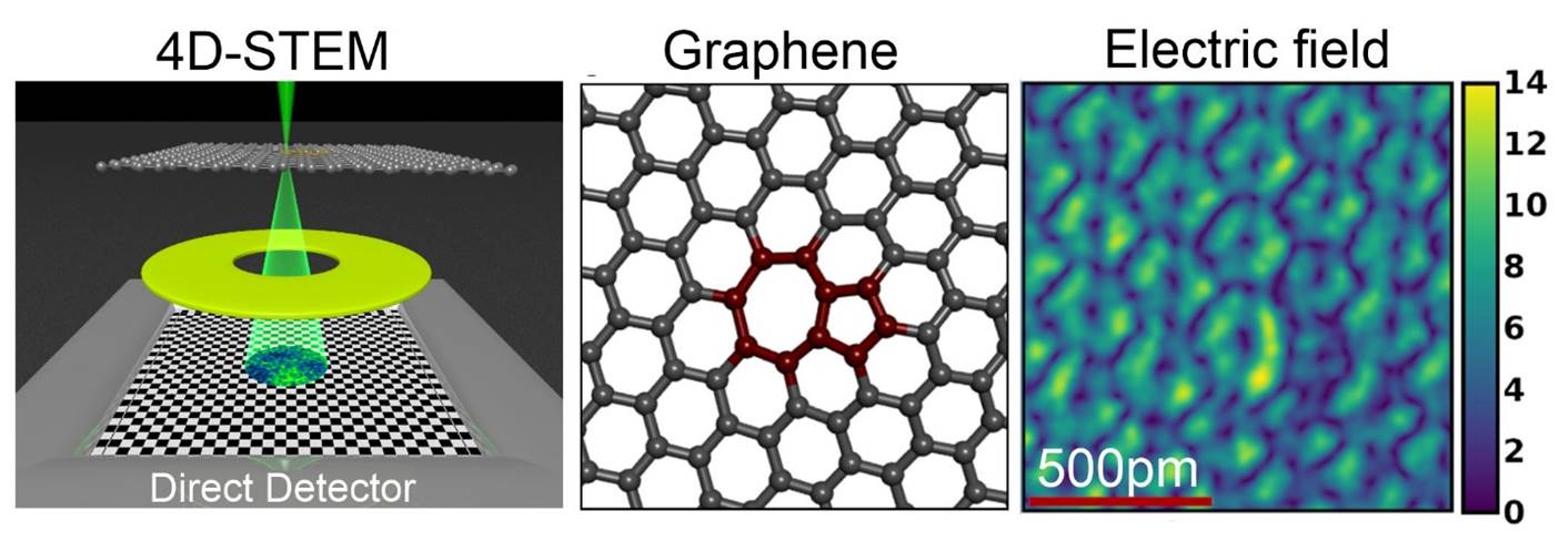
The authors focused on point dislocations in graphene due to their underlying role in plastic deformation and their high stability at elevated temperatures. By combining experimental data from 4D-STEM with first principles materials modelling using density functional theory, the authors were able to show that the asymmetry in the 5-7 dislocation core produces fluctuations in the local atomic density that modulates the electrostatic fields across nanoscale distances. 2D maps of the electric field magnitude showed increased values inside the heptagon core of the dislocation, Figure 1.
Surprisingly, the results showed that the electrons propagating through the material experience electrostatic effects from atoms that are beyond the nearest neighbors, providing some of the most detailed insights into atomic structure and bonding at the single atom level in solid-state materials. The research revealed that conventional TEM/STEM imaging approaches such as phase contrast TEM and annular dark field STEM were inferior to the new 4D-STEM approach that relies on measuring the quantum mechanical expectation value of momentum transfer to the electron beam as it interacts with the samples in-plane electric fields. These results provide important progress towards the goal of measuring spatial fluctuations of electron density in materials with picoscale resolution. The 2D material family provides an excellent testbed for probing fundamental behavior of high energy electrons with individual atoms and the development of methods that extend our ability to characterize structure and shed new knowledge on bonding in materials and the influence of defects.
In order the measure small electric fields in atomically thin materials, high quality data with excellent signal to noise is required, but this is extremely challenging because individual atoms have small scattering cross-sections and it takes time to accumulate counts above the background noise level. This requires stability of the sample in the electron microscope system, so it doesn’t move more than 50pm over a 3 minute period during data acquisition, all the while sitting at a high temperature of 700oC in-situ. This required innovation and engineering to advance in-situ heating chips with suspended graphene regions that were extremely stable at elevated temperature, and stable electron-optics in the TEM to raster-scan the focused 1Å electron probe slowly across the graphene and measuring the full electron scattering patterns from each atom in the sample. The team now seeks to extend this work to even higher sensitivities of electric field detections to then remove the contributions for positive charged nucleus, revealing the electron density and hopefully the valence electron distributions.